Products & Technologies
Products & Technologies
Services
Resources
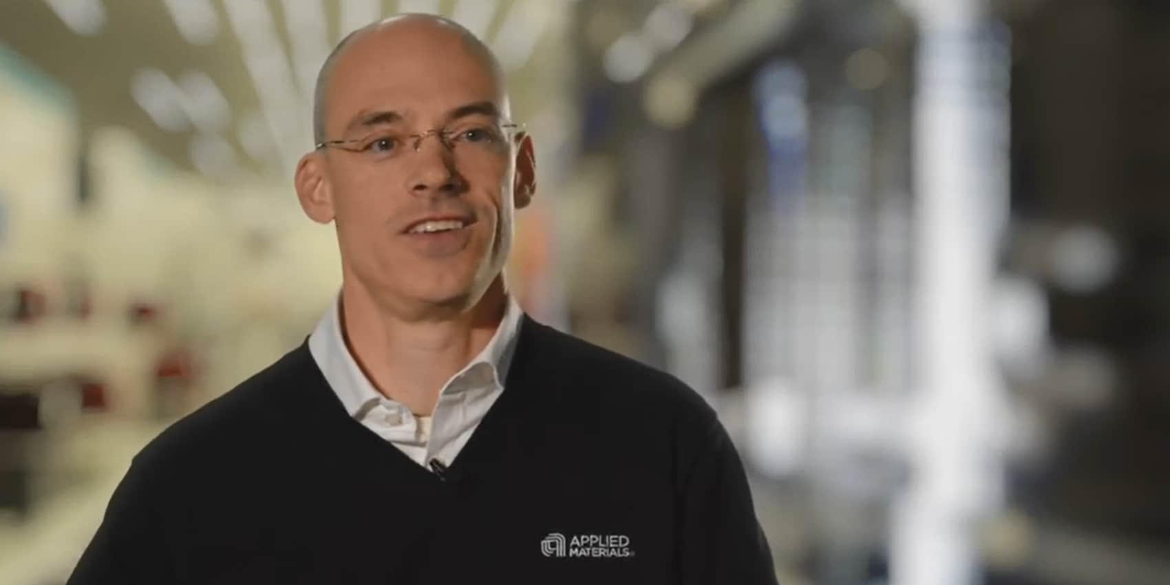
Chris Bencher
Office of the CTO
Chris Bencher is an influential technologist working in the CTO office at Applied Materials on path-finding and commercialization of advanced-patterning techniques. A respected industry expert, he has contributed to multiple products that have generated more than $1B in revenue, and provided technical innovation, diligence and leadership to guide the company’s roadmaps and develop new business opportunities.
Since he first joined Applied more than 20 years ago, Bencher has directed research and development in antireflective coatings, carbon hardmasks, double-patterning integration, and directed self-assembly. He also helped develop thin film and interface engineering solutions for the transition to dual damascene and supported the company’s entry into the lithography and advanced patterning markets. He is a leading advocate for the capabilities of sidewall-spacer double patterning, publishing annually and working with designers and electronic design automation (EDA) companies to further extend the self-aligned double patterning (SADP) technique for logic.
Before joining the semiconductor industry in the early 90s, Bencher graduated from Rensselaer Polytechnic Institute and the University of California, Berkeley with degrees in materials science.
He holds more than 57 U.S. patents for semiconductor manufacturing, including 20 in the field of patterning techniques and many of the earliest on SADP process flows. He participates on the International Technology Roadmap for Semiconductors (ITRS) lithography roadmap team, and co-chairs the Alternative Lithography conference at SPIE Advanced Lithography, where he also serves on the symposium executive committee.


