Products & Technologies
Products & Services
Company
Contact
Products & Services
Products & Technologies
Services
Resources
Company
Contact
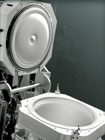
Endura® Underbump Metallization PVD
Applied Materials brings extensive PVD experience to back-end packaging, including NiV, Cu, Ti, TiW, CuCr, TaN, and AI, with proven solutions for UBM and bond pad. These solutions leverage Applied Materials' PVD expertise in advanced interconnect structures and world-class electrostatic chuck and preclean technologies to deliver thin films with excellent uniformity over a broad range of thicknesses (<1,000Å to >1µm).
Active wafer temperature control and stress modulation facilitate integration between interconnect metals and solder bumps with low cost of ownership and minimal die loss. In-situ removal of organic residues and native oxide using the Preclean XT ensures a clean surface that promotes low contact resistance and excellent adhesion.