Products & Technologies
Products & Services
Company
Contact
Products & Services
Products & Technologies
Services
Resources
Company
Contact
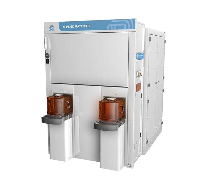
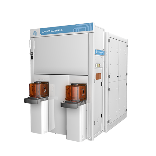
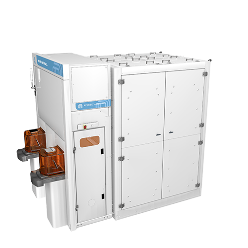
SEMVision G10 Defect Analysis
Defect review has always been an integral part of semiconductor fabrication, as the mechanism to monitor and control the quality of individual manufacturing process steps. With the continuous scaling of features, the size of the defects of interest (DOI) continue to decrease as well. These smaller defects directly impact device yield and demand extremely high-resolution imaging to detect and distinguish the defects from the process variation noise. Additionally, with the increasing complexity of device architectures, higher image resolution is needed not only to detect defects, but also to characterize them. This allows chip manufacturers to identify the root causes of problems and take corrective action for faster ramp and time-to-market.
The SEMVision G10 defect review system with novel cold field emission (CFE) technology offers industry-leading, sub-nanometer resolution to address many of today’s challenges. This unprecedented sensitivity is critical for a wide range of imaging capabilities, including both small surface-defects and buried defects. Elluminator™ technology has been an industry standard for back-scattered electron (BSE) imaging, see-through (ST) imaging and effective defect detection in high aspect ratio (HAR) structures. For un-patterned wafers, the G10 enables comprehensive, high-productivity review using an enhanced light source and optics capable of detecting defects <13nm. The SEMVision G10 also leverages and extends state-of-the-art automation solutions, enabling higher fab productivity and accelerating the ramp process to high volume manufacturing. A Purity™ ADC (automated defect classification) engine is powered by advanced machine learning capabilities to provide a high-purity and fully-classified Pareto chart of yield-limiting defects.
- 1 / 4
- 2 / 4
- 3 / 4
- 4 / 4