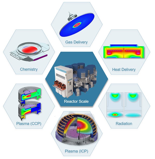
Reactor Scale​

Reactor Scale​

Novel architectures, materials, structures and packaging solutions are essential to address and enhance the power, performance, area, cost and time to market (PPACt) requirements of the semiconductor industry. The outcome is increased device complexity, placing greater demands on wafer fabrication equipment to achieve consistent, high-quality features across wafers and chambers while reducing operational costs and environmental impact.

ACE+ Suite solutions have made it possible to model complex reactors and a wide range of semiconductor manufacturing and packaging processes. These software solutions provide engineers the ability to simulate and analyze various aspects of the semiconductor manufacturing process, leading to improved efficiency, reduced costs and faster time to market for new products. Some of the key solutions include:​

Equipment Design and Optimization Modeling:​

  • Gas and electric delivery systems​
  • Heat and light delivery systems​
  • Thermal, chemical and plasma sources​

Process Characterization and Recipe Optimization Modeling​:​

  • Physical & chemical vapor deposition (PVD and CVD)​
  • Atomic layer deposition (ALD)​
  • Epitaxial deposition (Epi)​
  • Dry and wet etching processes​

Key ACE+ Suite capabilities used in semiconductor reactor scale modeling:​

  • Coupling to feature scale modeling​
  • Advanced and automated geometric modeling and meshing ​
  • Multi-species transport with gas phase and surface reaction modeling​
  • Electromagnetic and ICP, CCP and DC plasma discharge modeling ​
  • Monte Carlo radiation modeling ​
  • Parallel scalability, journaling, and scripting for workflow automation ​
  • Ysis tool​
reactor scale

Unleash innovation through simulation-driven exploration​