Back to Menu
VeritySEM® 5i Metrology
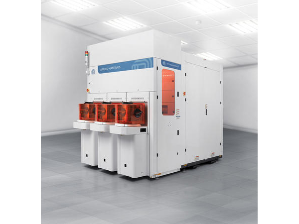
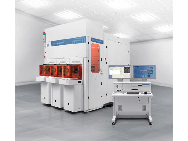
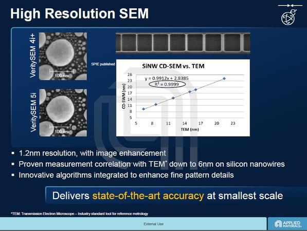
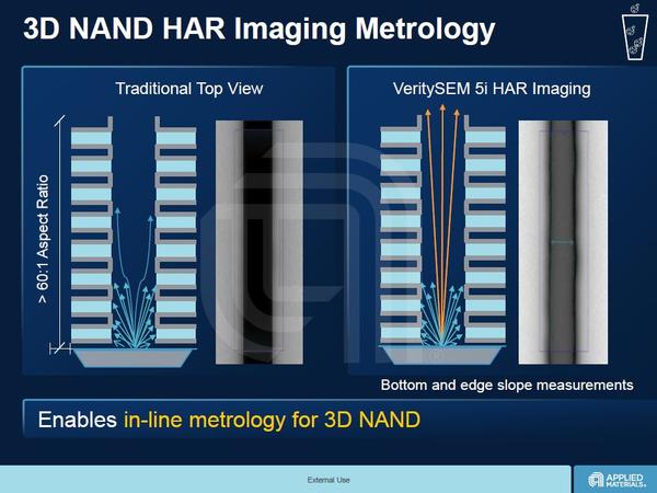
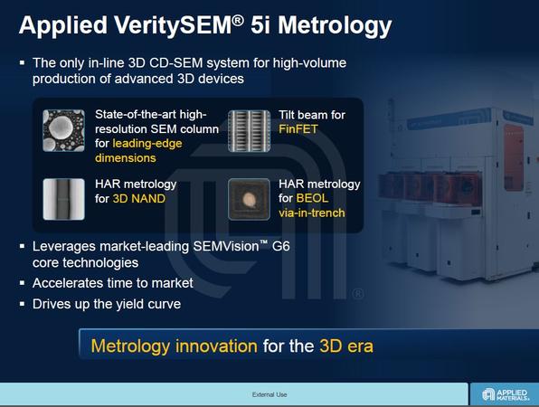
The newest in the Applied Materials VeritySEM product family, VeritySEM 5i CD-SEM system features first-of-its-kind, in-line, 3D capabilities for high-volume metrology of logic and memory devices at the 1xnm node and beyond. Leveraging market-leading SEMVision® G6 core technology, the new system addresses the unprecedented challenges in measuring physical dimensions posed by leading-edge geometries. Its state-of-the-art, high-resolution SEM column makes possible measurements as small as 6nm; innovative image enhancement algorithms aid measurement of fine pattern details. An in-column tilt-beam enables 3D FinFET metrology, while back-scattered electron (BSE) metrology addresses high aspect ratio 3D NAND structures, and BEOL via-in-trench bottom CD and characterization metrology.
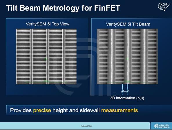
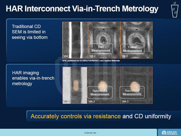
FinFETs challenge traditional metrology in such measurements as gate and fin heights, whose uniformity is critical to device performance and yield. Current in-line CD SEM technology can monitor only top-view dimension variations, not those in height and slope. The VeritySEM 5i system’s in-column beam tilt remedies these issues, enabling gate and fin heights to be calculated and controlled.As technology scales down, the aspect ratios of 3D NAND memory structures are increasing to 60:1 and beyond, making accurate measurement of the bottom CD impossible using conventional metrology. High-resolution BSE imaging enhances the signal received from within these structures, allowing the VeritySEM 5i system to “see” deep into vias and trenches for precision measurement. This capability also improves metrology for via-in-trench bottom CD in BEOL processing where the desired connectivity between underlying and overlaying metal layers must be achieved to minimize via resistance.
The VeritySEM 5i system’s exceptional in-line accuracy and process control eliminate more time-consuming and costly off-line wafer cross-sectioning while helping chipmakers to streamline process development, improve device performance and yield, and shorten ramp times to high-volume production.
The VeritySEM 5i system continues to offer hands free recipe creation and full automation. An offline recipe generator (ORG) features recipe editing capabilities via an external server, enabling multiple users to create recipes from computer-aided design offline without the need for wafers. The recipes are automatically stored in the tool database. By eliminating recipe creation time loss, the ORG enables the user to maximize the tool's utilization in production.
The tool's OPC|CheckMax is a proven solution for automating the optical proximity correction (OPC) mask qualification process. As scaling proceeds below 32nm, OPC-enhanced features are commonly incorporated into mask designs for all layers. Hundreds of CD measurements are required to verify that the features printed on the wafer are indeed what the device designers intended to produce. With a suite of proprietary algorithms, OPC|CheckMax receives input from electronic design automation systems, automatically creates CD-SEM measurement recipes, and then directs the VeritySEM 5i system to measure thousands of sites at high throughput without operator assistance.


- 1 / 8
- 2 / 8
- 3 / 8
- 4 / 8
- 5 / 8
- 6 / 8
- 7 / 8
- 8 / 8
