Products & Technologies
Products & Services
Company
Contact
Products & Services
Products & Technologies
Services
Resources
Company
Contact
Solar
Solar
Technology
Specialties
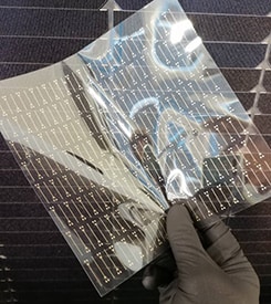
Printed Electronics
Advanced Processes
Applied Materials develops and manufactures complete solutions to address the ultimate technical challenges in printed electronics. We can support customers from feasibility studies with a dedicated process engineering team through proof-of-concept verification to prototyping. In parallel, the engineers will design and develop complete hardware solutions for your high-volume manufacturing needs.
The advanced process capabilities are also made possible thanks to the ecosystem built in more than twenty years of leadership in advanced screen-printing: from materials suppliers to screen/stencil manufacturers to research institutes and Universities, Applied will identify the proper solution to solve customers' high-value problems.
We offer a set of proprietary processes to accomplish the ultimate PE industry challenges, such as:
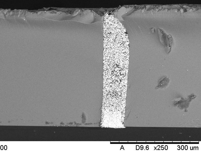
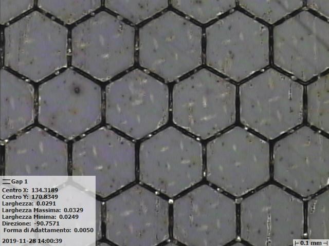
- Fine line printing down to 15 μm and line/spacing down to 30/30 μm
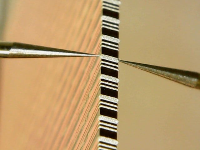
- Wrap around electrodes, or side wiring, entirely performed with screen printing
- High aspect ratio printing, enabled by our proprietary process of double and multiple printing
- High aspect ratio (up to 10) via filling
- Direct Patterning/Masking down to 30 μm
For more details, contact us at printed_electronics@amat.com.