Products & Technologies
Products & Technologies
Services
Resources
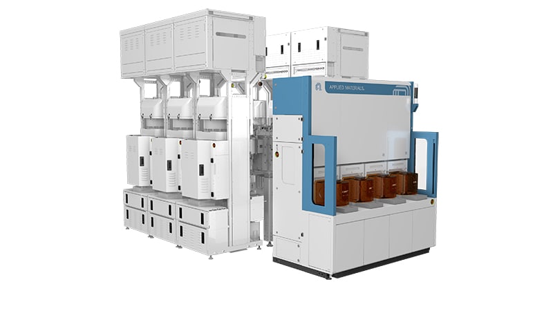
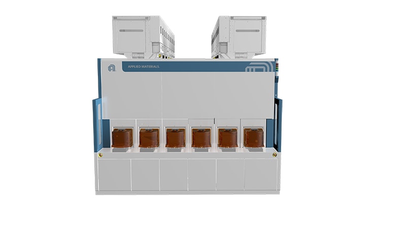
Applied Vericell™ Solar Wafer Inspection System
With the continuous development of photovoltaic industry, the efficiency of solar cells has been continuously improved from the early Mono & poly crystalline full-back-field cells to PERC cells, and now to TOPCon, IBC and HJT cells. The capacity of a single cell production line has increased from 25MW to 1GW now. With the improvement of production capacity and the iteration of technology, the demand for high-purity silicon wafers is increasing, which also requires equipment manufacturers to provide the most valuable equipment for the market with more fast, accurate and powerful capability.
At the same time, for the cost reduction of solar cell, the size of silicon wafer is getting bigger and bigger year by year. Wafer thickness changed from 150μm to 80μm, with the change of more and more big and thinner, wafer become more fragile, and they are more vulnerable to defectivity and breakage. The requirements for the wafer inspection equipment have absolutely risen to a very high level, too. Vericell is the first tool in the world to inspect G12 wafer.
Through long-term cooperation with TCL Zhonghuan, Chinese tiger 1 silicon wafer enterprise in China, Vericell has continuously provided the market with newer, more accurate and faster silicon wafer inspection and sorting equipment from generation to generation. This equipment has reduced the hardware investment and operation cost of customer, and the high accurate test results have provided strong help for customers' upstream process traceability. This value is reflected in constantly assisting customer to improve their yield and providing strong guarantee for customer to be invincible in the market.
In view of the large wafer size, thinner and higher productivity of silicon wafers, how to take six high-resolution photos of four 210*210 silicon wafers in one second and capture all defects, which brings unprecedented challenges to the data processing ability of equipment, stability of transmission conveyor, the cooperation between camera and light source, etc. Based on the advanced industry foresight and actual R&D ability in the past years, together with upstream and downstream suppliers, the latest generation Vericell GT equipment is perfectly manufactured, which not only meets the requirement of existing customer, but also provides the most reliable data support for tracking defective process and improving process parameter.
According to the physical and electrical property of silicon wafer, we can detect items including wafer size, thickness, warp, surface edge chip, side edge chip, chamfer edge chip, saw mark, resistivity, stain, TTV, ucrack, pinhole and carrier lifetime.
Available for dual lanes HCWs (TPT 18000 WPH@ HCW)
Available wafer thickness ≥90μm
AI and deep learning to maximize the detection rate and purity of classification.
The most robust tool in the industry to process variation.
Machine can support coin stack, cassette loading and unloading.
Machine can connect Industry 4.0 robot or automatic packaging machine and assembly line.
Have full automation at both ends -load and unload to allow operator free factory and drive down total COO.
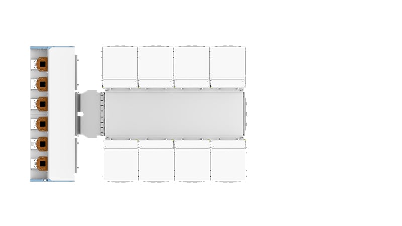
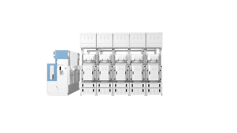
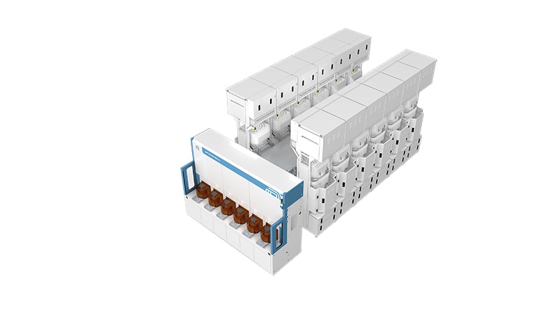
The smallest footprint provides the maximum speed and throughput, and the single unloading outlet will simplify the connection with the packaging assembly line. The mature Industry 4.0 solution provides the possibility for the factory to be intelligent factory without lights on, and MES provides system support for the unified management of the factory.
What our equipment pursues is to ensure to provide customers with the most accurate inspection result based on the premise of maximum speed. High-precision inspection results can better ensure the delivery quality and reduce the probability of customer complaints.
If the accuracy of our inspection result is 0.1% higher than that of any other competitor, the factory with 10 million wafers daily output can reduce the annual loss of 3.65 million wafers. At the same time, if the 0.1% is tracked back to the upstream process and the make the process improved, the factory can make an extra profit of 3.65 million wafers every year.
Silicon wafer factory: If you want to become a world-class supplier of silicon wafer, the result of high-precision inspection is the most effective tool to improve the yield and quality.
Cell factory: If you want to maximize the yield of cell production line, it is the best choice to eliminate the defects of silicon wafers before going into the line, reduce the process cost caused by defective silicon wafers in the production line and improve the overall yield of cell.
We are never compromised on performance- not when we transitioned from small to large wafers, and not when we boosted TPT by factor 2 within less than 3 years. All these changes came with maintaining the same sampling rate and pixel size as the small and slow tools.
- 1 / 5
- 2 / 5
- 3 / 5
- 4 / 5
- 5 / 5
