Products & Technologies
Products & Services
Company
Contact
Products & Services
Products & Technologies
Services
Resources
Company
Contact
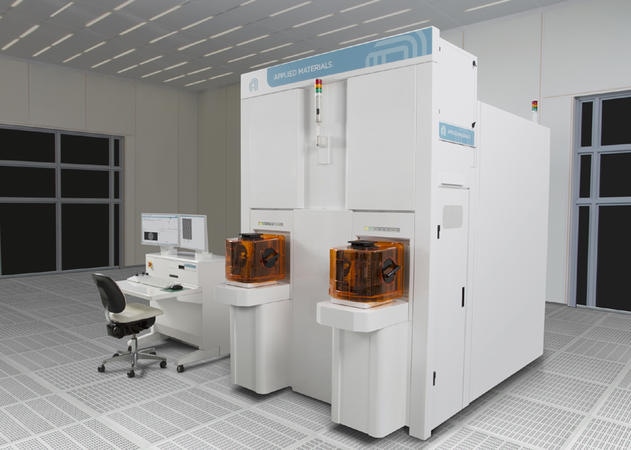
PROVision® 3E eBeam Metrology
As semiconductor features continue scaling and device architectures become denser and more complex, fabrication processes involve more steps and process control limits become tighter. Traditional optical metrology is leading to measurement deficiencies that are making it more difficult to correlate intended patterns with on-die results. As a result, today’s leading-edge chip designs require a new class of metrology that goes beyond optical target-based approximation, statistical sampling, and single-layer control.
The PROVision 3E system combines nanometer resolution, high speed, and through-layer imaging to produce the millions of datapoints needed to correctly pattern today’s most advanced designs, including 3nm foundry-logic chips, GAA transistors, and next-generation DRAM and 3D NAND. With these capabilities, it sees beyond the blind spots of optical metrology, performing accurate measurements across the wafer and between the many layers of a chip to generate the multidimensional data sets needed to achieve the best chip performance and accelerate time to market.
The system’s industry-leading ebeam column technology features the highest electron density available, enabling detailed imaging at 1nm resolution at a rate of 10 million accurate, actionable measurements per hour. Applied’s unique Elluminator® technology captures 95 percent of back-scattered electrons to quickly measure critical dimensions and edge placement at multiple levels simultaneously. A broad range of ebeam energies encompasses high-energy modes for rapid measurement hundreds of nanometers deep and low-energy modes for damage-free measurement of fragile materials and structures, including EUV photoresist. Applied’s decades-long CD SEM and algorithm expertise ensure accurate and precise measurements of critical features.
With its innovative technical features, the PROVision 3E system improves yield, saves production costs, and shortens time-to-market.