半导体 (Semiconductor)
技术
-
ALD
-
CMP
-
CVD(化学气相沉积)
-
ECD
-
外延生长
-
刻蚀
-
离子注入
-
测量与检测
-
Pattern Shaping
-
光掩膜
-
PVD(物理气相沉积)
-
快速热处理(RTP)
-
模拟
-
化合物半导体
-
微机电系统(MEMS)
-
功率
晶圆制造厂环境解决方案
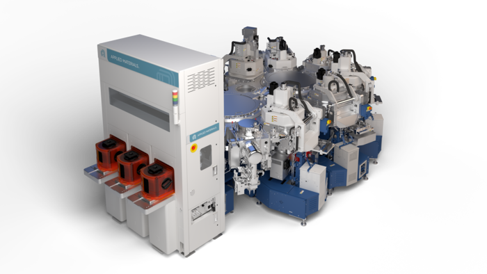
Endura™ Impulse™ PCRAM PVD
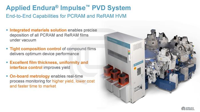
应用材料公司的 Endura Impulse PVD 系统是用于相变随机存取存储器 (PCRAM) 和电阻式随机存取存储器 (ReRAM) 器件大规模量产 (HVM) 且具有生产价值的集成材料解决方案(Integrated Materials Solution™)。 PCRAM 和 ReRAM 是新兴的非易失性存储器,可填补 DRAM(用于数据处理)和 NAND(用于数据存储)之间不断扩大的性价比差距。 PCRAM 和 ReRAM 可以提高存储和检索的速度、用电效率和可靠性,即使在断电时也能保留软件和数据。
The Impulse system consists of up to seven deposition chambers integrated with pre-clean, anneal, and degas chambers. Leveraging Applied’s extensive expertise in PVD, the deposition chambers employ several proven Applied PVD technologies to deposit with exacting precision the compound materials that boost data read speeds with low power consumption. As the volume of data being generated worldwide expands exponentially and power required for processing these data by artificial intelligence applications increases, fast data access and low-power computing are becoming a priority.
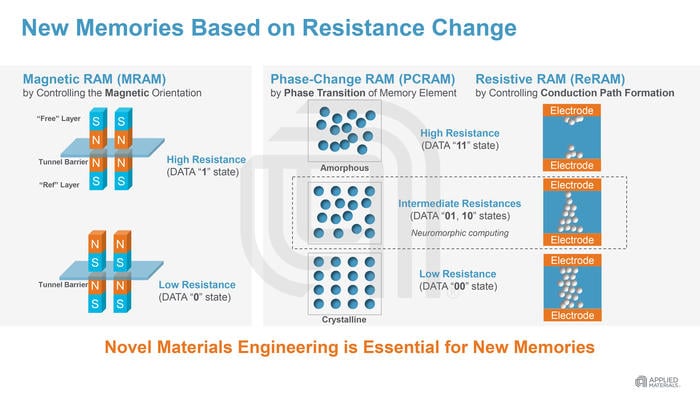
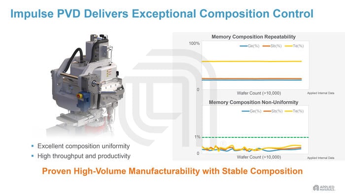
Specialized Impulse GST PVD chambers deposit the compound phase-change material that transforms from a high-conductance amorphous state to a low-conductance crystalline state when exposed to heat via an electrical current. This material is a form of chalcogenide glass composed of germanium (Ge), antimony (Sb), and tellurium (Te), hence the acronym GST. The chamber’s superior GST density promotes device speed and prolonged endurance. Similarly, different versions of Impulse chambers are optimized to deposit metal oxide and nitride materials with exceptional control of thickness and composition uniformity as resistive memory materials for ReRAM application.
The system’s Avenir™ RF PVD chamber deposits the ovonic threshold switch (OTS) layer, typically a compound of Ge, arsenic (As), and selenium (Se) that also changes from conductive to resistive, depending on voltage. OTS is the leading choice for selector material in PCRAM and ReRAM. This chamber has been enhanced to produce the dense, amorphous film necessary for precise threshold voltage and off-state control. Further, automatic capacitance tuning achieves extreme composition uniformity within this layer--essential for memory reliability and lifetime—while magnet arrangement effectively controls thickness uniformity across the wafer. A software-controlled, integrated passivation kit facilitates safe and cost-effective maintenance of the OTS chamber with high productivity.
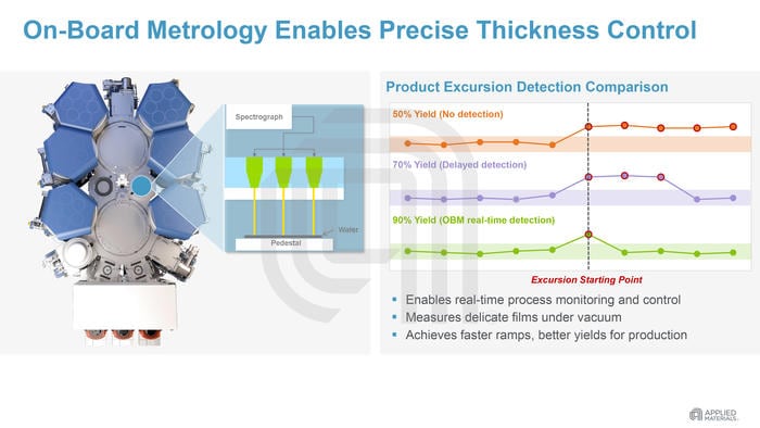
To ensure that film thickness remains within tight specifications, the system includes on-board metrology to measure the critical GST and OTS layers as the stack is created. These measurements are extremely accurate (to 0.2 Angstrom) as the film properties from which the thicknesses are derived have not been altered or degraded by removing the wafer from vacuum. Real-time, layer-by-layer monitoring allows rapid detection of process excursions, which helps improve yields, lower cost, and accelerate time to market—key considerations for HVM.
- 1 / 5
- 2 / 5
- 3 / 5
- 4 / 5
- 5 / 5
Read about the Applied Endura Clover MRAM PVD system.