Products & Technologies

Products & Services
Company
Contact
Back to Menu
Products & Services
Products & Technologies
Services
Resources
Company
Contact
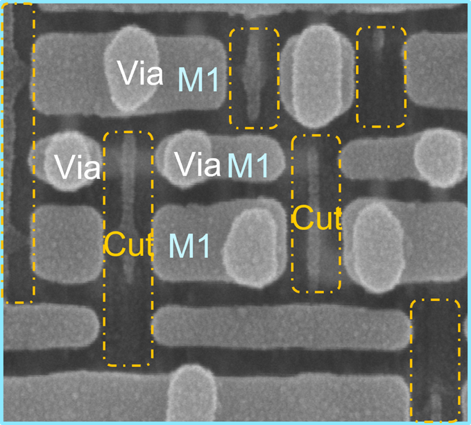
Patterning Control
Patterning Control is a series of critical metrology steps used to ensure that the right material dimensions, locations, and compositions were created and shaped on the wafer.
With today’s complex device architectures, it is impossible to create transistors and interconnects without in-line metrology that measures and provides feedback on the actual critical dimension sizes and placement, ensuring new structures perfectly align with the structures of previous process steps.
Applications range from process window development and qualification during early stages of development, to high sampling of in-line critical dimensions, on-wafer uniformity, hot spot characterization, and overlay measurements. Through such applications, device manufacturers accelerate time-to-market, ensure yield levels, and gain predictability to their device performance and reliability in early stages of the manufacturing process.