Products & Technologies

Products & Services
Company
Contact
Back to Menu
Products & Services
Products & Technologies
Services
Resources
Company
Contact
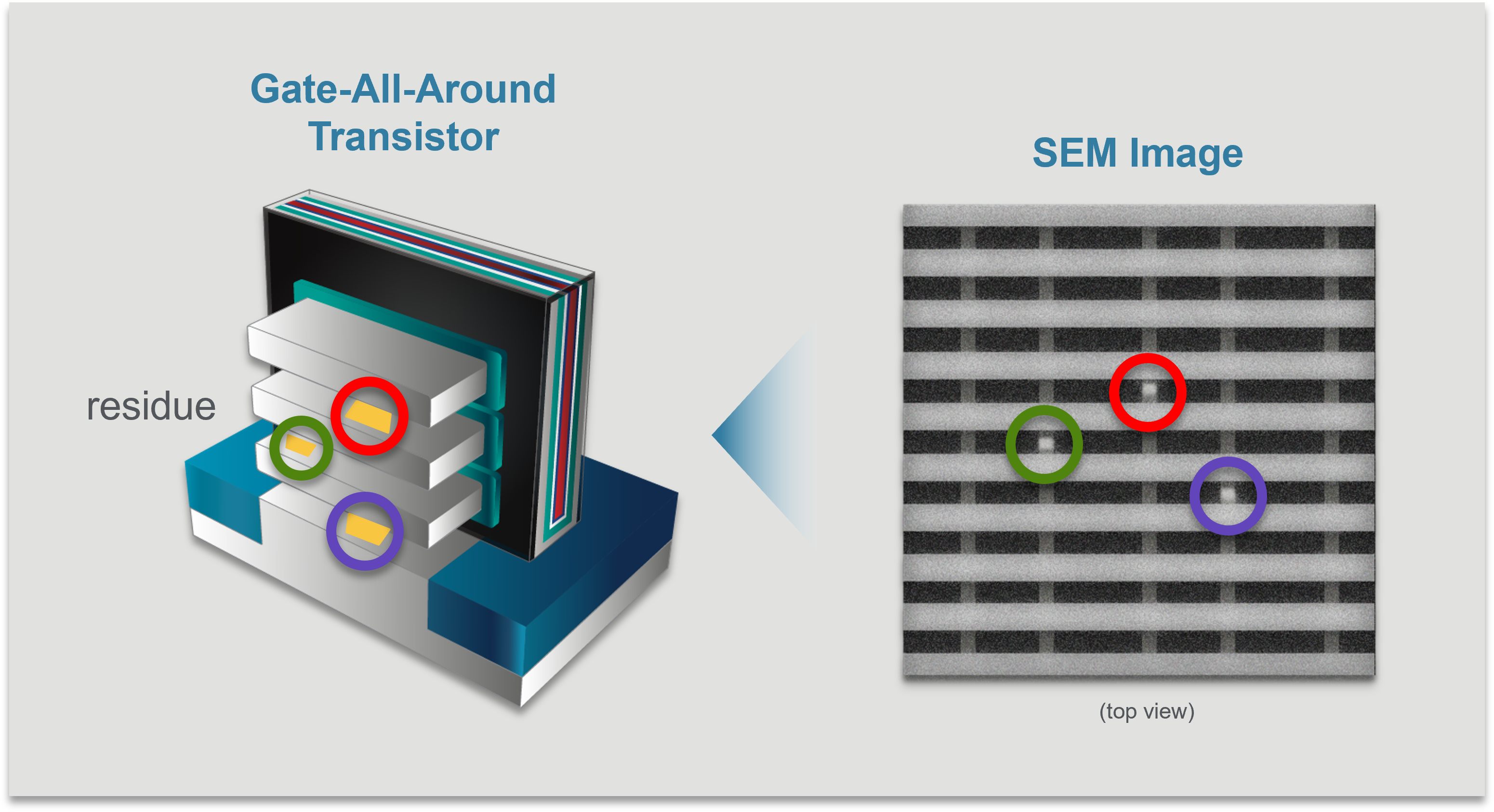
Defect Control
Defect Control involves the monitoring of wafers at critical steps in the fabrication process, allowing early identification and real-time resolution of process excursions without impacting fab yield and productivity.
Common defects include particles, residues, scratches, bridges and shorts.
During early stages of R&D, device manufacturers need to characterize their process and focus on small, yield-limiting process or integration defects found on wafers and reticles. At this stage, high sensitivity to small surface/buried defects is critical and drives the adoption of high-sensitivity eBeam inspection solutions that image key areas of interest.
During ramp and high-volume manufacturing, fabs requires tight control of any excursion defects. The variety of defect types and sizes has grown significantly with the increasing complexity of device architectures and smaller process windows, resulting in ‘mix-and-match’ sampling strategies that balance sensitivity, speed and cost.