半導體 (Semiconductor)
Endura® ALPS® PVD (ALPS Co & Ni)
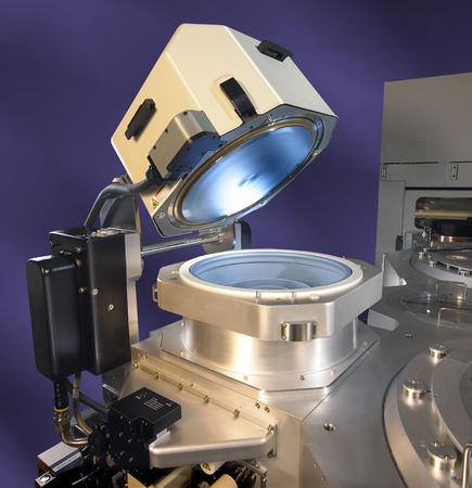
The Applied Endura ALPS (Advanced Low-Pressure Source) Cobalt PVD (Physical Vapor Deposition) system offers a simple, high-performance silicide solution for gate and contact applications in high aspect ratio structures. Extending cobalt to ≤90nm technology nodes, ALPS technology produces good Co bottom coverage with no plasma damage to the device and very low defect counts. Endura ALPS Co addresses the challenges of titanium agglomeration, contact resistance change, and dopant suction through excellent resistivity, low leakage current, and thermal stability.
For logic and memory applications at 65nm/55nm and below, silicon consumption by Co and roughness of the Co silicide/silicon interface become more critical. The Endura ALPS Ni PVD system delivers stable NiSi films with 2x less silicon consumption, smoother film interfaces, and lower resistivity. ALPS Ni achieves bottom coverage of 100Å without plasma damage to the device while minimizing particle counts.
The Applied Endura ALPS Ni PVD system features single-chamber Siconi Preclean interface engineering technology to address the surface preparation challenges of cleaning silicon prior to the formation of NiSi. Siconi Preclean provides a highly selective clean (>20:1 SiO2:Si, >5:1 SiO2:SiN) without the need for the tight queue time control between clean and Ni deposition required with conventional HF clean processes. By generating the etchant in a remote plasma source, damage to the substrate is significantly reduced, resulting in minimal etching of features such as nitride spacers and the silicon gate. In addition, device studies show fewer NiSi2 spike defects and improvement in junction leakage with the Siconi Preclean compared to conventional HF dip process flows.

