半導體 (Semiconductor)
Cobalt Product Suite
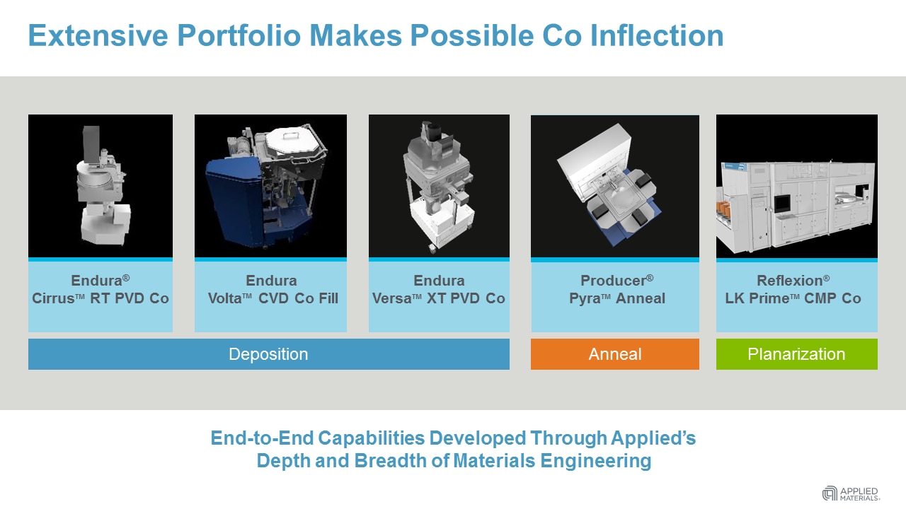
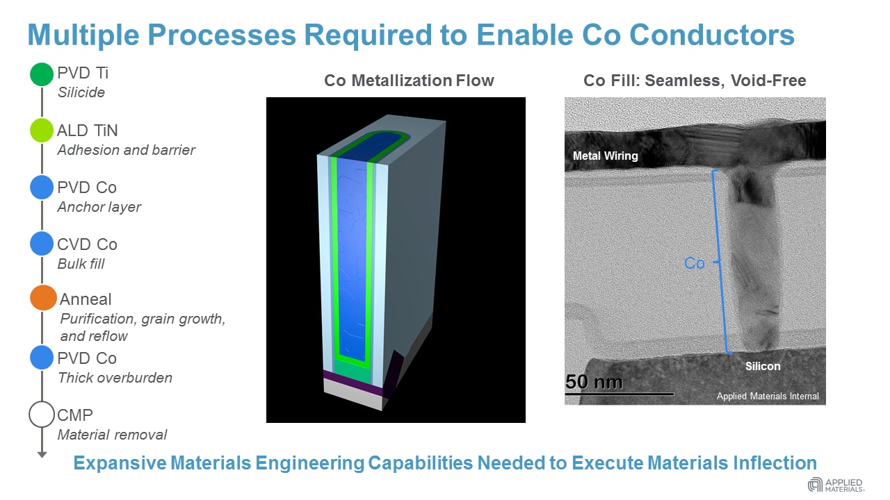
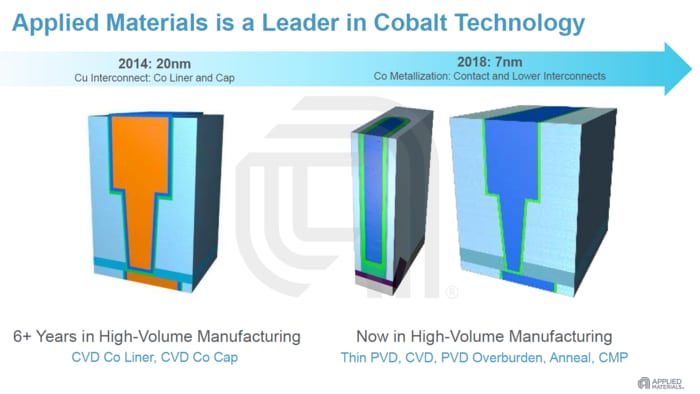
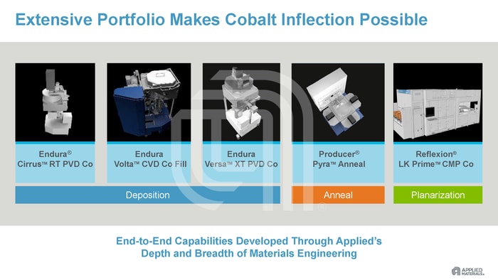
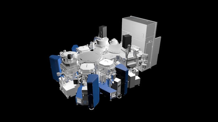
Applied Materials continues to extend its technical leadership in metallization, introducing the most significant material innovation in contact and interconnect since copper was introduced for dual damascene 20 years ago. Three new deposition processes are complemented by a new anneal product and a production-proven CMP tool to comprise an end-to-end process suite (illustrated below) that makes it possible to use cobalt as a conducting material and thereby sustain high-performance logic transistor and interconnect scaling.
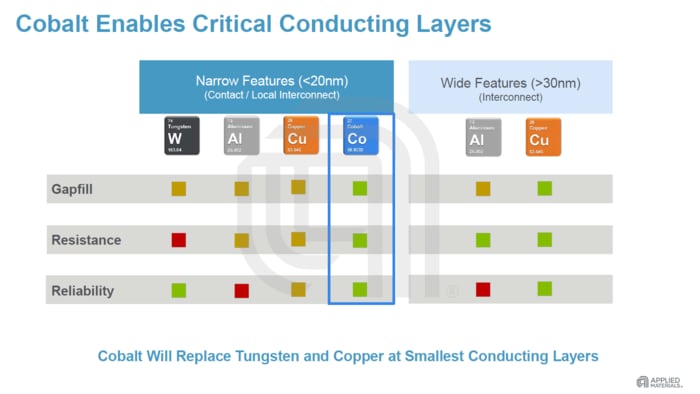
As feature CDs continue shrinking, lowering device power consumption and improving performance speed are increasingly limited by the performance of the contact and the local interconnects. For the 7nm node and beyond, the increasing resistance in tungsten gapfill results in higher power consumption and slower chip performance. First-level copper interconnects face similar challenges as resistance rises with decreasing copper volume, also slowing chip performance.
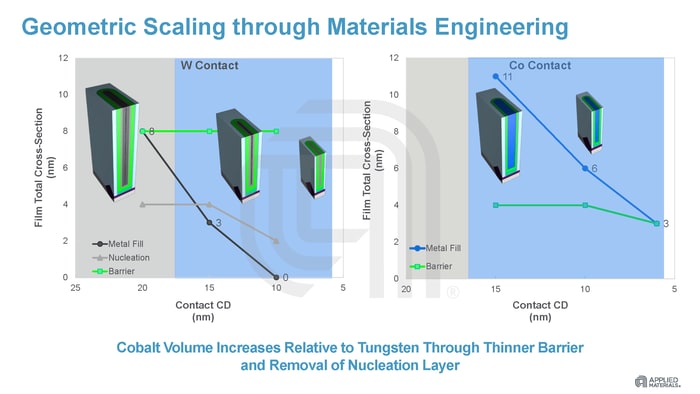
Not only is cobalt an inherently a lower-resistance material than tungsten, but the process flow for creating cobalt contacts also results in greater a volume of conducting metal, which improves performance, and in an associated reduction in variance, which improves yields. Similarly, in interconnect, cobalt demonstrates better line and via resistance scaling and less electromigration than copper, facilitating higher current densities.
- Applied Endura Cirrus RT PVD Cobalt: This system deposits the initial thin layer of cobalt to which the subsequent CVD cobalt adheres.
- Applied Endura Volta CVD Co: This system deposits the cobalt fill following the PVD layer. The seam created by this deposition process is subsequently eliminated during the anneal step.
- Applied Endura Versa XT PVD Co: This system deposits the thick overburden following the anneal step.
- Applied Producer Pyra Anneal: This system heats the wafer, causing cobalt reflow that eliminates the seam in the bulk fill, enlarges the grain size, purifies the cobalt, and reduces the resistance. To read more about this system, click here.
- Applied Reflexion LK Prime CMP: Using slurries specifically optimized for polishing cobalt, this system removes the overburden produced by earlier deposition steps and creates a planar surface for subsequent process steps. To read about this system, click here.
- 1 / 5
- 2 / 5
- 3 / 5
- 4 / 5
- 5 / 5
