
半导体 (Semiconductor)
解决方案与软件
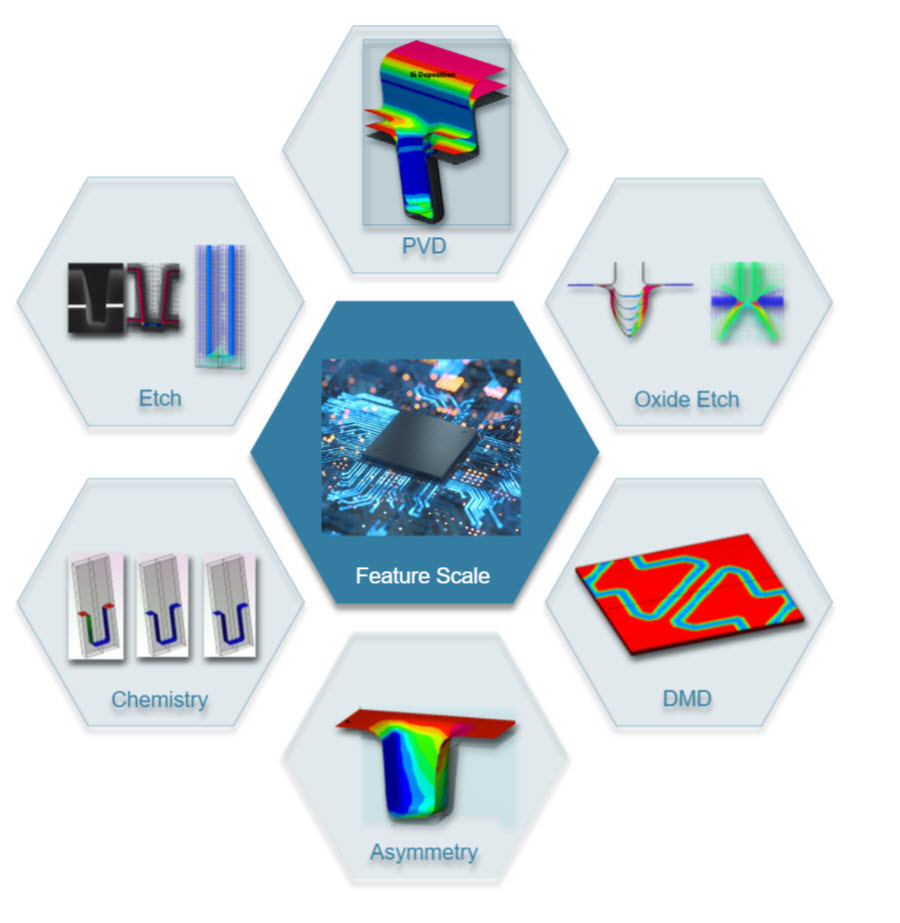
Feature Scale
Feature-scale models play a critical role in understanding the topographical evolution of features on semiconductor wafers during thermal, chemical and plasma processing. Evolution of these features across the wafer is dependent on the uniformity of thermal and chemical environment over the wafer. By leveraging feature scale models, coupled with reactor scale models from ACE+, chip makers can gain deeper insights into the topographical evolution of features and optimize their process recipes to achieve improved uniformity, higher yields and greater process control.
TOPO+ is a level-set-based 2D and 3D feature-scale modeling software that simulates the transient surface evolution during etching and deposition processes on nano-meter scale features across a wafer or semiconductor device. TOPO+ uses ballistic transport of the gas species and complex surface chemistry in different etch, sputter and deposition processes including three-dimensional topological evolution for multiple materials and multi-processes steps. It can directly integrate species fluxes (neutral, radical, ion), ion energy and angle distribution functions across the wafer from ACE+ reactor scale simulation.
Key TOPO Applications:
- Metal Deposition (Al, Cu, W, Ti)
- Barrier Layer Deposition (TiN, TaN)
- High-k Dielectric Deposition
- Epitaxial layer Deposition
- Silicon Dioxide, Silicon Nitride Deposition
- Contact/Via Etching
- Gate Etching
- Interconnect Etching
- Dielectric Etching
- Deep Trench Etching
- Shallow Trench Isolation
Key TOPO+ capabilities:
Fast automated and adaptive meshing
Two and Three-dimensional
Incorporates deposition and etch processes
Multiple materials and complex surface chemistries
Fully integrated with CFD-ACE+ importing flux, Ion energy and angular distribution from reactor scale model
Parametric DOE capability