Centris® Sym3® Y Etch
Semiconductor scaling continues steadily into the single-digit nodes, setting increasingly demanding requirements for precision and uniformity in chip fabrication. At earlier nodes, when features were larger, a greater range of variation in etch depth, line or space width, or profile angle could be accommodated without affecting device performance. Similarly, occasional particles remaining on feature surfaces did not jeopardize device reliability. At today’s advanced nodes, however, the slightest differences in etch depth, line or space width, or profile angle can be fatal flaws. And defect-free surfaces are equally essential.
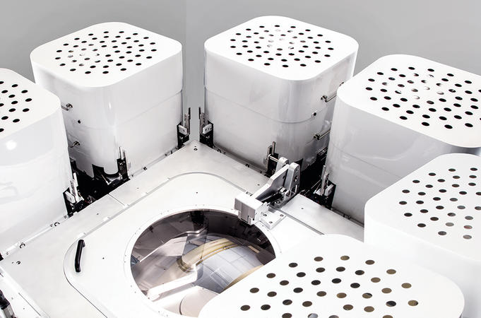
Leveraging the exceptionally successful Centris Sym3 product design and refining it for critical conductor etch and EUVL patterning applications at leading-edge memory and foundry-logic nodes, the highly versatile Centris Sym3 Y is now Applied’s most advanced etch system. The combination of a high-conductance chamber architecture with the innovative pulsed RF source technology achieves outstanding etch profile control by quickly and efficiently exhausting the etch byproducts that can accumulate with each wafer pass.
Extremely high etch selectivity allows sequential etching of multiple layers of different materials in a single chamber as well as the exceptional depth and profile control required to create densely packed, high-aspect-ratio structures, including FinFETs and emerging gate-all-around transistors. Manufacturing defects are reduced and wafer yield is improved with a new proprietary coating that protects critical chamber components during the etch process. Die-to-die variability across the wafer is reduced with a novel electrostatic chuck, and extreme edge of the wafer yield is improved with active edge control.
The Sym3 Y system consists of multiple etch chambers and plasma clean wafer processing chambers that feature system intelligence software to ensure that every process in every chamber matches precisely, enabling repeatability and high productivity for high-volume manufacturing.
With unmatched process uniformity and defect control, the Sym3 Y system offers customers new ways to shape and pattern materials, enabling new 3D structures and new ways to continue 2D shrinking even as chip features become tighter and smaller, aspect ratios greater, and materials more complex at advanced nodes.