製品・サービス
Back to Menu
製品・サービス
トレンド
Quantum Breakthroughs Begin with Materials
アプライドマテリアルズとCEA-Letiが共同研究施設を拡張、特殊用途向け半導体のイノベーションを推進
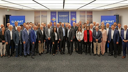
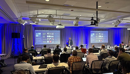
Applied Materials Convenes Semiconductor Leaders in Europe

Applied Materials Announces Cash Dividend