Products & Technologies

Products & Services
Company
Contact
Back to Menu
Products & Services
Products & Technologies
Services
Resources
Company
Contact
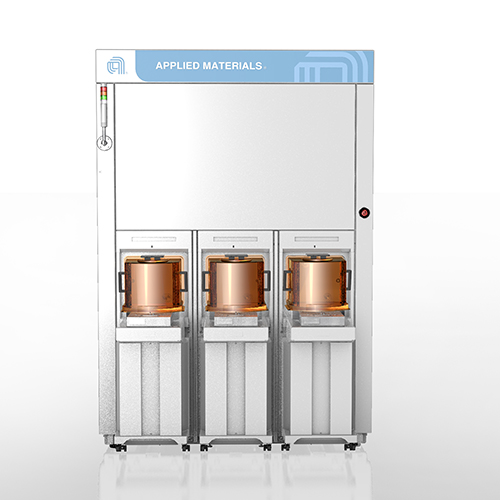
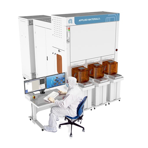
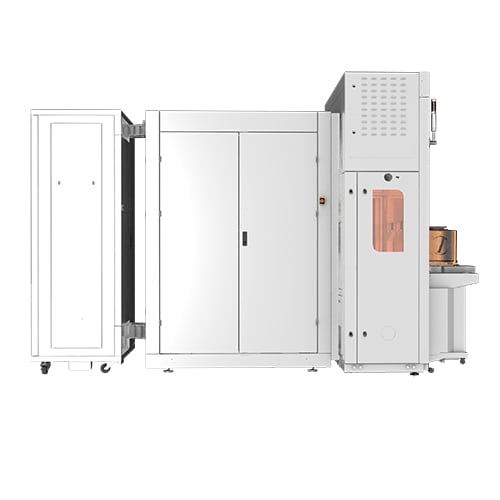
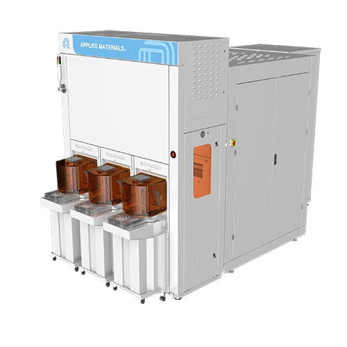
VeritySEM® 10 Critical Dimension (CD) Metrology
When it comes to measuring semiconductor device patterns, the CD-SEM (critical dimension scanning electron microscope) is often called “the ruler of the fab” because it produces the most precise, sub-nanometer measurements available. CD-SEMs are used to measure the critical dimensions of patterns, such as lines and spaces, once the lithography scanner transfers them from mask to photoresist. These measurements continuously calibrate the scanner and process to ensure the patterns are correct before they are etched into the wafer. Measuring the critical dimensions of device features becomes more challenging as photoresists get thinner with EUV and especially high-NA EUV. We need thinner photoresists to enable mask patterns to be developed with the 10X fewer photons available as compared to deep UV. Also, thinner resists help prevent the densely packed lines formed with EUV from collapsing into one another. When moving to high-NA, the resists become even thinner to compensate for the depth of focus loss of the high-NA EUV scanner.
The Applied VeritySEM® 10 CD-SEM metrology platform is specifically designed to measure the critical dimensions of features patterned with EUV and high-NA EUV. The system uses industry-leading sub-nanometer eBeam resolution to quickly capture between 13 and 36 precise CD measurements across the wafer. The increased resolution and scan rate enable faster EUV scanner calibration which helps customers accelerate process recipe development, maximize yield in HVM, and increase ROI from their large lithography module investment. Low landing energy is used to minimize interaction with the thinner and more delicate photoresists of EUV and high-NA EUV in order to preserve pattern fidelity while maintaining tight metrology production requirements.
VeritySEM 10 also brings enhancements to gate-all-around (GAA) transistors and 3D NAND memory metrology. Leading back-scattered electron (BSE) technology with a new detector architecture is used for 3D metrology and the extremely high aspect ratio features of GAA, enabling up to 50% tighter matching and higher resolution eTilt imaging. 3D NAND devices with increasing staircase interconnects can take advantage of specially-optimized working points with efficient secondary electron (SE) collection and advanced algorithms that increase the accuracy and robustness when imaging the CDs at the bottom of these deep structures. Additionally, a large field of view (LFOV) image generation capability combined with higher depth of focus permit complete 3D NAND staircase metrology with tighter matching and precision.
The VeritySEM 10 joins the VeritySEM family and a fleet of over 1,400 systems worldwide. VeritySEM is the pioneer of BSE technology with the highest-resolution SEM column currently available in high volume manufacturing.
- 1 / 4
- 2 / 4
- 3 / 4
- 4 / 4