Products & Technologies

Products & Services
Company
Contact
Back to Menu
Products & Services
Products & Technologies
Services
Resources
Company
Contact
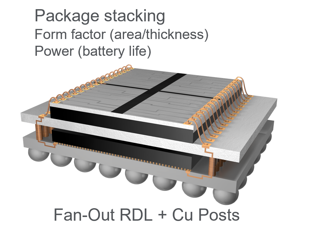
Fan-Out
In conventional technologies, package size is usually considerably larger than the die size. Establishing a connection between the tightly spaced die connection pads and the outside world has been the primary function of this packaging.
In flip chip ball grid array packaging, such connection pads are distributed on the chip surface and the chip is flipped for connection, limiting the area of bonding bumps to the chip area. With advanced technology nodes, this also means that the bump pitch would no longer be compatible with PCBs.
Fan-out packaging was developed to relax this limitation. It provides a smaller package footprint along with improved thermal and electrical performance compared to conventional packages and allows an increased number of contacts without increasing the die size. In fan-out wafer level packaging (WLP), the wafer is diced first, then the die are re-positioned on a carrier wafer (or panel), with space for fan-out kept around each die. The carrier is then reconstituted by molding, followed by building a redistribution layer atop the entire molded area. Processing substrates with polymers in vacuum tools require special care due to their tendency to degas and to pollute the existing layers.

Applied’s products that enable fan-out technologies include our Endura PVD, Charger PVD, and Nokota ECD tools. Our Endura and Charger tools feature specific chambers to guarantee process cleanliness and the best contact resistance.
More information on this topic can be found on our Master Class and blogs.