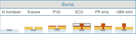
Bump
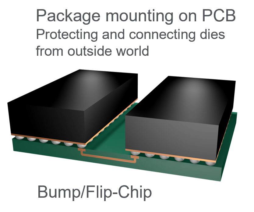
Apart from wire bonding, bumping is the most established technology for chip-to-chip, chip-to-substrate, and substrate-to-PCB connections. Bumping requires forming raised regions of metal over bonding pads to allow the simultaneous bonding of the "bumps" to a substrate or a package. There are different levels of bumping, each with a different resolution, from a coarse pitch (500um and up) to a very fine pitch (<50um). Getting devices closer to each other to increase data transfer rate and reduce power consumption requires smaller and smaller bump diameter and pitch, without sacrificing yield.
The desire to extract more system level performance at even lower power is leading designers to consider how to best integrate chips and systems. Designers are finding it difficult to place the transistors they need for high-performance computing, machine learning and inferencing on a single die. As an alternative approach, designers are using multi-die advanced packages that enable high-performance logic and memory in closer proximity, which reduces latency and power consumption. This approach called heterogeneous integration requires an extremely high density of short connections, orders of magnitude higher than offered by previous packaging technologies.
Applied Materials products that enable bump technologies include our Endura PVD, Charger PVD, Nokota ECD and Raider ECD.
More information on this topic can be found on our Master Class and blogs.