Products & Technologies

Products & Services
Company
Contact
Back to Menu
Products & Services
Products & Technologies
Services
Resources
Company
Contact
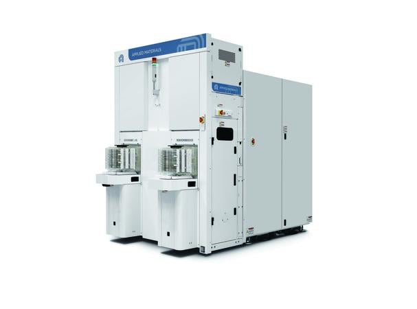
SEMVision® G7 Defect Analysis
Defect review, classification, and analysis are vital in semiconductor fabrication as the means to monitor and control the quality of individual steps in the manufacturing sequence. Shrinking feature dimensions and the growing complexity of semiconductor devices demand constant enhancement of imaging capabilities to rapidly identify critical defects of interest that are also shrinking and whose locations in 3D structures are more challenging to see. High-resolution images of defects to determine their character; speedy, accurate classification and composition analysis; and reliable determination of root causes are essential in enabling chipmakers to establish precise statistical process control, ramp up production runs rapidly, and achieve consistently high production yields.
To meet these demands, the Applied SEMVision G7 system offers greater imaging variety and advances in automatic defect classification (ADC) based on expanded machine learning capabilities. Besides the imaging capabilities of the previous SEMVision generation, the new system offers unique imaging of the wafer-edge bevel and apex where undetected defects can reduce device yield. To achieve robust review of unpatterned wafers, an enhanced light source and collection mechanism combined with improved noise suppression enable optical detection of defects as small as 18nm.
The new system leverages and expands Purity® ADC capabilities. This market-leading technology was the first to correctly identify different types of yield-limiting defects in a production environment using advanced algorithms that dynamically “learn” the numerous defect classes and a statistical classification engine that achieves benchmark classification accuracy and repeatability. Purity II features algorithms that enhance machine learning to sustain system accuracy, consistency, and reliability for longer periods than are typically achievable in dynamic process environments. A new critical defect prioritization algorithm ensures that defects of particular interest are represented in the pareto charts that highlight the relative preponderance of each defect type so that corrective actions can be implemented in order of importance.
In addition, Purity II also adds automatic engineering analysis to these machine learning capabilities. Classifying defects using both SEM images and computer-aided design data produces more precise location-based classification that facilitates faster, more accurate root cause analysis and yield prediction. This performance in turn results in shorter cycle times and higher productivity—especially critical for foundries, where good yields must be achieved rapidly for thousands of new chips each year.