Products & Technologies

Products & Services
Company
Contact
Back to Menu
Products & Services
Products & Technologies
Services
Resources
Company
Contact
Endura® CuBS RF XT PVD
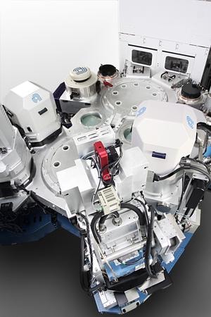
The Applied Endura CuBS (Copper Barrier/Seed) RF XT PVD system serves logic and memory applications at the 3x/2x node and beyond. The SIP (Self-Ionized Plasma) EnCoRe II Ta(N) barrier and EnCoRe II RFX Cu seed process chambers feature high-ionization PVD technology that delivers full-coverage, low-temperature film deposition, with minimal overhang and smooth morphology.
The thickness tuning capability of the EnCoRe II Ta(N) chamber enables customers to reduce barrier thickness for line resistance scaling to the 3x/2x nodes while reducing electromigration and stress migration through superior bottom and sidewall coverage. For the Cu seed layer, the EnCoRe II RF XT Cu chamber employs innovative magnetron motion, flux control, and a high resputter ratio regime to further enhance conformal coverage. These technologies mitigate issues such as end-of-line voids at the wafer edge or post-CMP defects that degrade the quality of metal gap fill.
To address the increasing importance of interfaces as geometries shrink, Applied offers various preclean technologies to ensure interface integrity without adversely affecting critical dimensions or material properties. The Endura CuBS RF XT system features the innovative Aktiv Preclean, a breakthrough cleaning technology for efficient removal of polymeric residues and reduction of CuO while protecting porous low-k inter-level dielectric films, such as Black Diamond II. Unlike conventional reactive preclean methods, the Aktiv Preclean process results in no significant change in k value, thus enabling the transition to next-generation low-k dielectrics.
The Applied Endura CuBS RF XT PVD system sequentially deposits the Ta(N)/Ta barrier followed by the Cu seed layer under high-vacuum conditions. Integration of the complete sequence, including the preclean, on the Endura platform ensures excellent film adhesion and oxide-free interfaces, while preserving k value integrity for low via resistance and high device reliability.