Products & Technologies

Products & Services
Company
Contact
Back to Menu
Products & Services
Products & Technologies
Services
Resources
Company
Contact
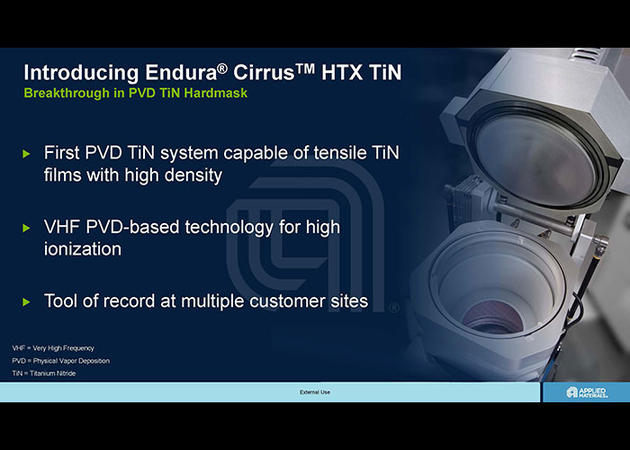
Endura® Cirrus™ HTX PVD
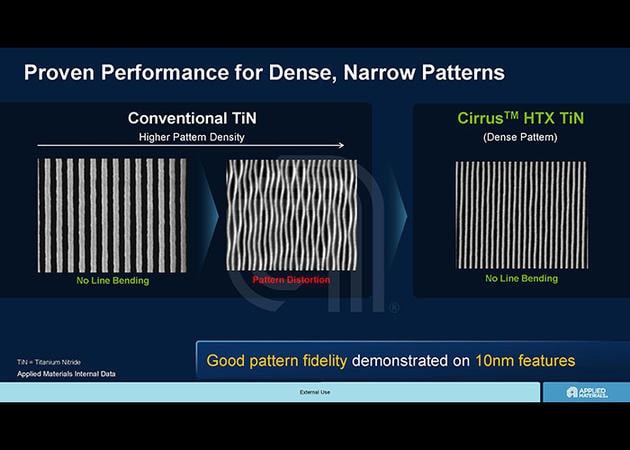
Revolutionizing physical vapor deposition (PVD) technology for titanium nitride (TiN) thin films, the Endura Cirrus HTX TiN solves hardmask extendibility challenges for next-generation devices. As chip features continue shrinking, innovations in hardmask are crucial for accurately patterning ever more complex, tiny interconnect structures. Leveraging years of expertise in PVD, the new system produces a breakthrough hardmask that ensures pattern fidelity beyond the 10nm node.
As chip designs advance, features are becoming progressively smaller with higher aspect ratios and are being packed more densely in creating advanced integrated circuits. Consequently, the robustness of materials used to define the patterns etched and metallized to create the circuitry (or interconnects) is vitally important in preserving the integrity of those patterns. The slightest flaw can make it impossible to properly metallize the device, rendering it unreliable or non-functional.
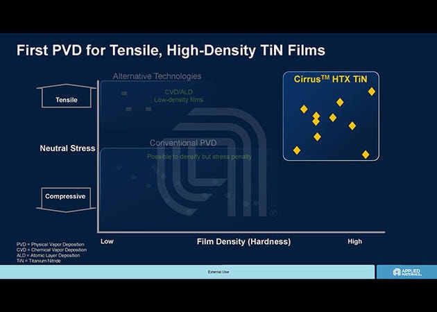
Titanium nitride (TiN) has been the standard hardmask material used to pattern low-k dielectric when fabricating interconnects. However, as the dielectric has gradually been made more porous to lower device capacitance at advanced nodes, it has become more fragile and susceptible to post-etch distortion (line bending and pattern collapse) caused by the compressive stress of the overlying TiN mask. Easing this natural compressive stress reduced film density—essential for withstanding the etch process.
- 1 / 6
- 2 / 6
- 3 / 6
- 4 / 6
- 5 / 6
- 6 / 6
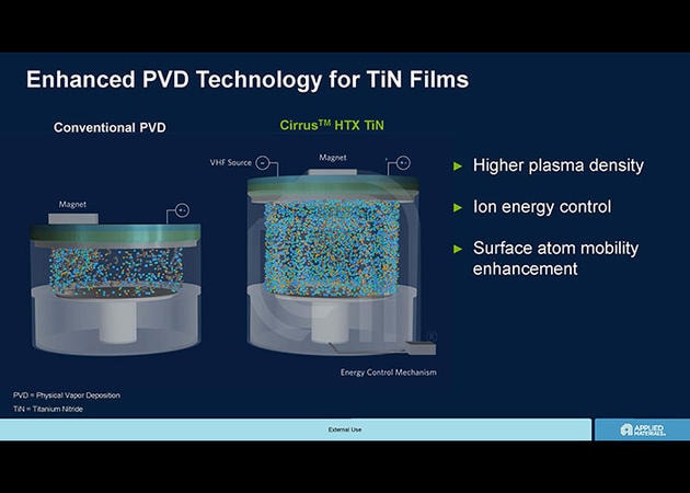
In a major breakthrough, the Endura Cirrus HTX PVD system employs a very-high-frequency RF source to achieve highly ionized plasma that facilitates modifying the film’s crystalline orientation, thus resolving the vexing tradeoff between stress and density. The resulting TiN achieves the ideal combination of tensile stress and high density that results in superior etch selectivity, excellent CD line width control and via overlay alignment, and fidelity of dense complex patterns. Combining exceptional film thickness uniformity with low defectivity further enables the new system to minimize variability and produce exceptionally precise patterning.
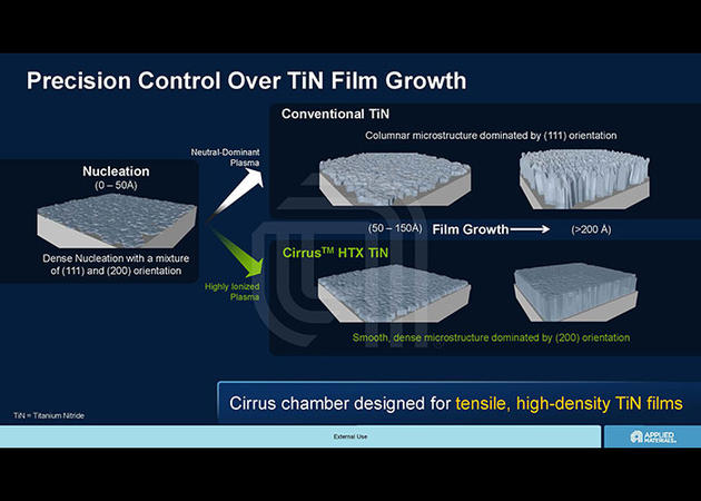
Compressive stress of conventional TiN leads to line width variation and pattern collapse in dense, complex interconnects.
High-density, tensile Cirrus™ TiN produces tight line width control and via overlay alignment to preserve the pattern integrity of dense, complex interconnects.
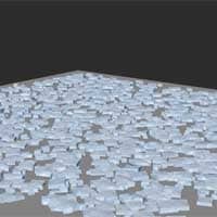
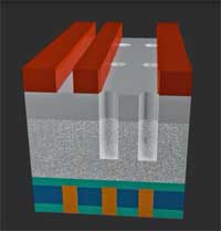
The crystal growth mechanism in conventional TiN results in voids between crystals and a rough top surface.
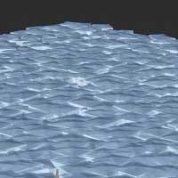
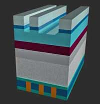
The crystal growth mechanism in Cirrus TiN results in void-free film and a smoother top surface.