Products & Technologies

Products & Services
Company
Contact
Back to Menu
Products & Services
Products & Technologies
Services
Resources
Company
Contact
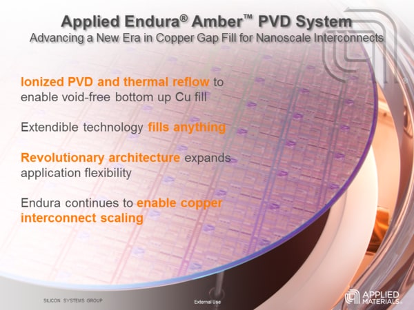
Endura® Amber™ PVD
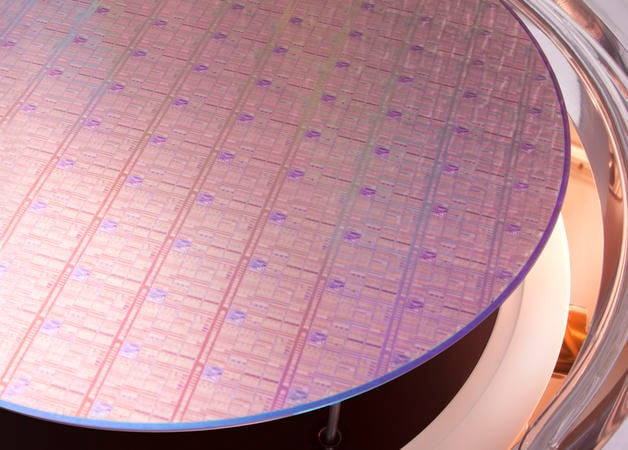
Reliable and complete filling of interconnect trench and via structures with copper is vital for device reliability in microelectronic fabrication. Essential steps in this process are the depositing of a barrier (to prevent copper diffusion into the surrounding insulating material) and a copper seed layer that facilitates subsequent electrochemical deposition (or plating) without voids or seams.
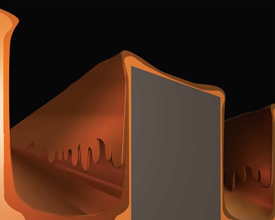
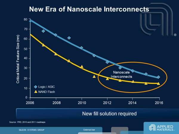
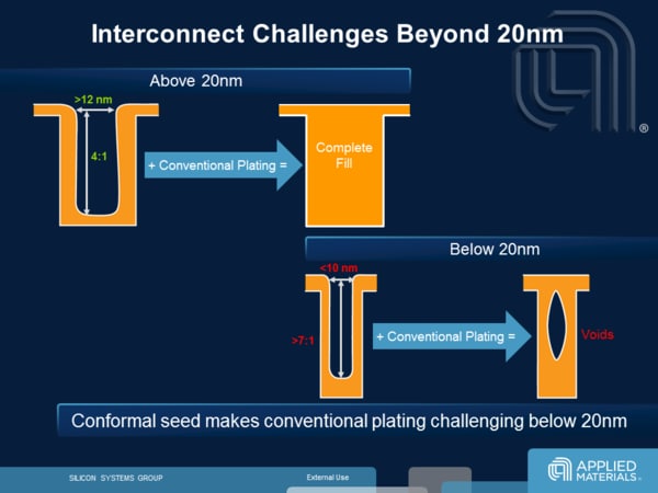
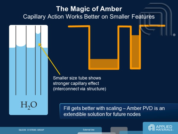
To date, ionized physical vapor deposition (PVD) has been able to achieve the required thickness and continuity of coverage on all surfaces for electroplating. Beyond the 2xnm node, however, even the most optimized barrier/seed process, showing conformal coverage without any overhang, creates feature aspect ratios unmanageable for electroplating.
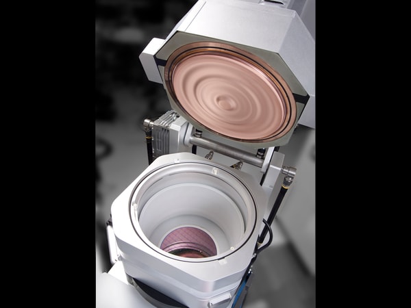
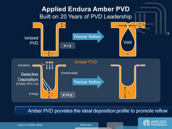
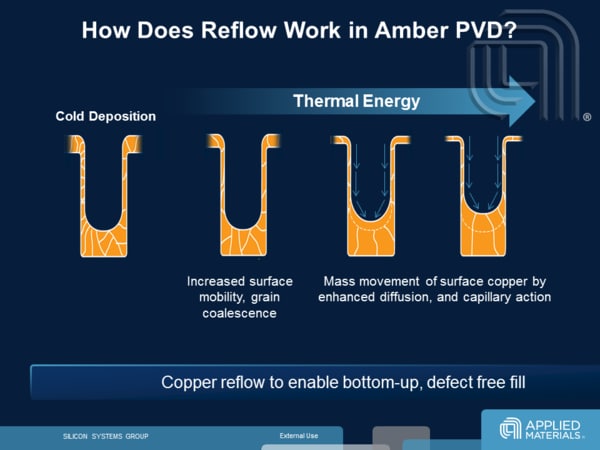
The unique Endura Amber PVD system resolves this difficulty with a proven all-in-one method that combines cold deposition and high-temperature thermal copper reflow to supersede EnCoRe II RFX copper seed technology. Copper overhang around the openings of ultra-small vias at the 1xnm node precludes conventional PVD from achieving the sidewall and bottom seed layer coverage required for optimal electroplating. The new system extends the current technology by augmenting PVD deposition with copper reflow to enable bottom-up fill. This two-step technique makes electroplating easier by either reducing the effective aspect ratio of the vias (when applied once) or completely filling the vias (when iteratively applied). It thus increases the surety of the void-free fill necessary for device reliability. Independent temperature control for each step of the deposition/reflow cycle offers flexibility for successfully integrating this process with a variety of liner materials.
This innovative copper seed technology is integrated on the Endura platform with pre-clean and EnCoRe II Ta(N) barrier technologies under high-vacuum conditions to enable high device yields in volume production.

Sundar Ramamurthy shows how revolutionary Amber PVD copper reflow addresses interconnect scaling challenges beyond 20nm.
- 1 / 10
- 2 / 10
- 3 / 10
- 4 / 10
- 5 / 10
- 6 / 10
- 7 / 10
- 8 / 10
- 9 / 10
- 10 / 10