Products & Technologies

Products & Services
Company
Contact
Back to Menu
Products & Services
Products & Technologies
Services
Resources
Company
Contact
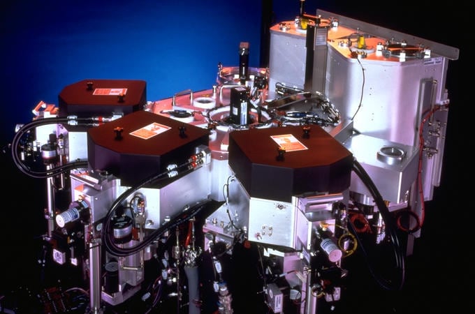
Centura® DXZ CVD
Applications in the advanced CMOS and MtM segments are driving the need for advanced 150mm and 200mm CVD technology. Ultra-thick oxides (≥20µm); low-temperature processing (<200°C); conformal, low wet-etch-rate films; and doped films with tunable refractive indices are needed to meet manufacturing requirements for these device technologies. These films join the broad portfolio of processes available on the Centura DXZ CVD system, from TEOS, silane-based oxides, and nitrides to low-k dielectrics, strain engineered, and litho-enabling films.
The DXZ CVD system is equipped with enhanced capabilities for handling a variety of MtM substrates (including SiC wafers) reliably and carefully from load lock wafer mapping to clear wafer orientation to wafer placement.
The Centura DXZ system design offers significant improvements in cost (e.g., process kit with zero consumable parts), throughput, ease of serviceability, and reliability. With single-wafer, multi-chamber architecture, the system delivers TEOS and SiC throughputs of up to 80wph (3,000Å PE TEOS and plasma silane) and USG throughput of up to 35wph (2000Å SACVD USG). Symmetrical design and small chamber volume promote efficient gas utilization for both deposition and clean chemistries, contributing to a low overall cost of ownership.