Products & Technologies

Products & Services
Company
Contact
Back to Menu
Products & Services
Products & Technologies
Services
Resources
Company
Contact
AKT®-PECVD System for Amorphous Silicon Application
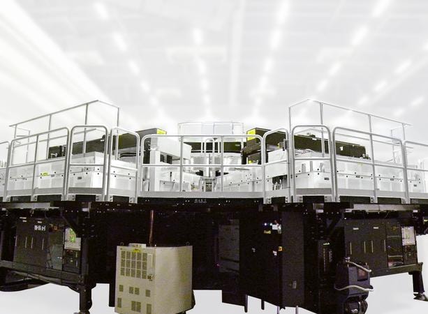
The industry-leading Applied AKT-PECVD platform deposits insulating films on large-area glass substrates for the fabrication of liquid-crystal display (LCD) screens. Applied Materials’ plasma enhanced chemical vapor deposition (PECVD) systems are used by virtually every major thin film transistor - liquid crystal display (TFT-LCD) manufacturer in Korea, China, Taiwan and Japan.
AKT-PECVD systems offer processes for both amorphous silicon (a-Si) and metal oxide (MOx) backplane technologies. Available films include both doped and undoped (a-Si), silicon oxide (SiOx), silicon oxynitride (SiON), silicon nitride (SiN), and in-situ multi-layer depositions.
Applied’s advanced PECVD technology provide a rapid, cost-effective path to bring metal oxide transistor technology to market, an emerging technology for manufacturing next-generation ultra-high resolution displays. Applied’s PECVD silicon oxide films provide a dielectric layer interface for metal oxide transistors that minimizes hydrogen impurities to improve transistor stability and provide optimized screen performance.
Proprietary process chamber technology enables AKT-PECVD systems to deliver excellent film uniformity and electrical properties over the complete range of glass sizes used in the display industry from Gen 2 (0.2m2) all the way up to Gen 11 (9.9m2).