Products & Technologies

Products & Services
Company
Contact
Back to Menu
Products & Services
Products & Technologies
Services
Resources
Company
Contact
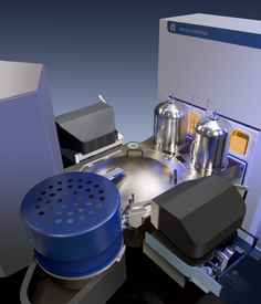
Atomic Layer Deposition (ALD)
ALD is a crucial enabler across multiple device segments, including today’s most advanced planar devices and the industry’s transition to 3D architectures. ALD also is being adopted across ICAPS for a range of uses, including passivation, encapsulation, and optical functions.
The ALD process builds up material directly on the surface of the chip, a monolayer at a time, to produce the thinnest, most uniform films possible. The self-limiting nature of the process and the related capability for conformal deposition are the basis for its importance as a scaling and 3D enabler. The self-limiting surface reaction makes atomic-scale deposition control possible: film thickness depends only on the number of reaction cycles performed. Surface control makes the films extremely conformal and uniform in thickness, both essential properties in emerging 3D device designs. ALD can also deposit high quality films at low temperatures, enabling new integration schemes and functions that would not be possible using other techniques. Applied’s ALD systems deposit a variety of oxides, metal nitrides, and metals on the wafer to create ultra-thin layers in advanced transistor (FinFET), memory, interconnect, CIS, optoelectronics, power, and RF applications.