Products & Technologies
Products & Services
Contact
Back to Menu
Products & Services
Products & Technologies
Services
Resources
Contact
Enabling Next‑Generation Devices
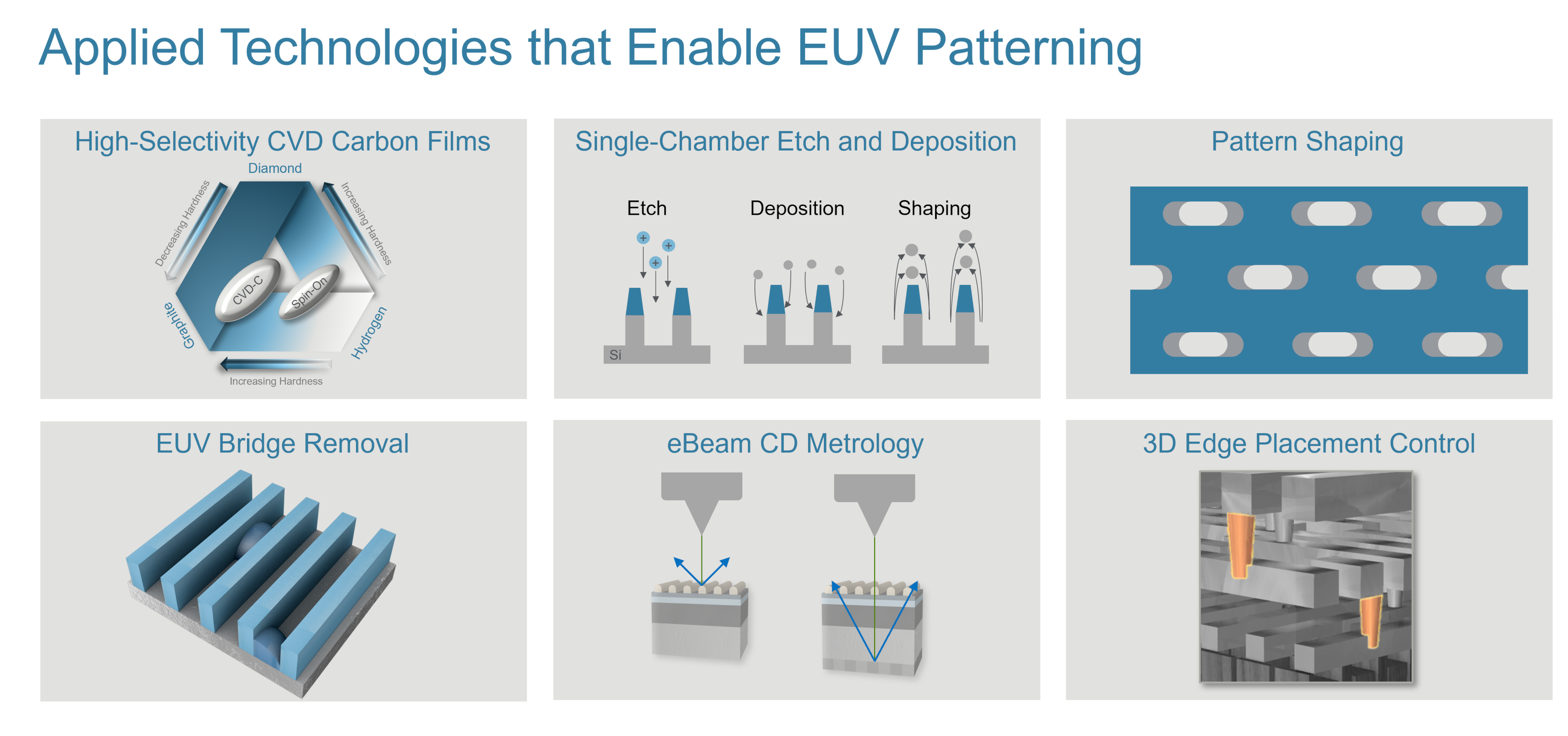
Over the years, lithography advances and materials engineering techniques evolved together to help us shrink features and increase density. Extreme ultraviolet (EUV) was a big step forward, giving us the ability to create 25nm features with a single litho pass. Today, we need even smaller features, and EUV double patterning is already being used. For the future, high numerical aperture (high NA EUV) is on the roadmap to replace EUV double-patterning with a single litho pass.
A number of materials engineering innovations need to happen to enable EUV scaling to continue, including replacing softer spin-on deposition films with more etch-resilient films. The Stensar™ Advanced Patterning Film helps customers tune EUV hard mask layers for specific thicknesses and etch resiliency, so they can achieve near-perfect EUV pattern transfer uniformity across the entire wafer.
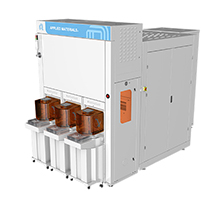
The lower number of photons in EUV creates stochastic errors, which create variability in the lines, spaces and vias being patterned. The smaller the EUV patterns, the larger the stochastic errors in the features we are trying to make. Applied's Sym3® Y Etch System enables customers to etch and deposit materials in the same chambers to heal stochastic errors and improve EUV patterns before they are etched into the wafer.
EUV double patterning is a technique commonly used to produce higher device density with tighter tip-to-tip spacing. While double patterning is effective at increasing feature density, it adds design and patterning complexity along with process steps that consume time, energy, materials and water—and increase the cost of wafer fabs and wafer production. The Sculpta® Pattern Shaping System helps chipmakers shrink designs without double patterning while also reducing energy and materials used in the process.
EUV photoresist is thinner and more delicate than DUV resists. If we used conventional eBeam systems to look for stochastic defects and measure the critical dimensions and overlay, we could distort the patterns on the delicate resist. To help customers inspect more thoroughly during the after-development and after-etch stages of EUV, Applied's VeritySEM® CD Metrology System uses lower energy to minimize interaction with the resist and a unique technology to improve EUV pattern image resolution, giving us sharp dark and light contrasts at low energy.
Prior to EUV, edge placement was much easier, where features were larger and alignment of the optical scribe lines allowed us to properly align layers. However, the optical proxy targets are at least 10 times larger than the features we are creating with EUV. Also, iterative process steps like double patterning introduce variations, and 3D designs create stresses and interlayer distortions. The PROVision® eBeam System allows engineers to see and measure edge placement through all EUV layers at the same time.