Products & Technologies
Products & Services
Contact
Products & Services
Products & Technologies
Services
Resources
Contact
Vantage® Vulcan® RTP
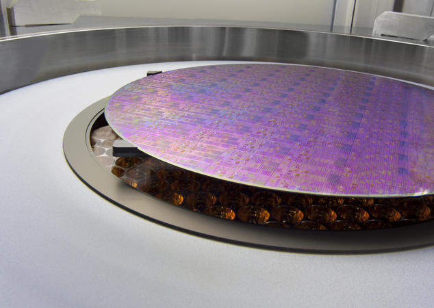
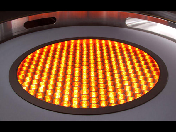
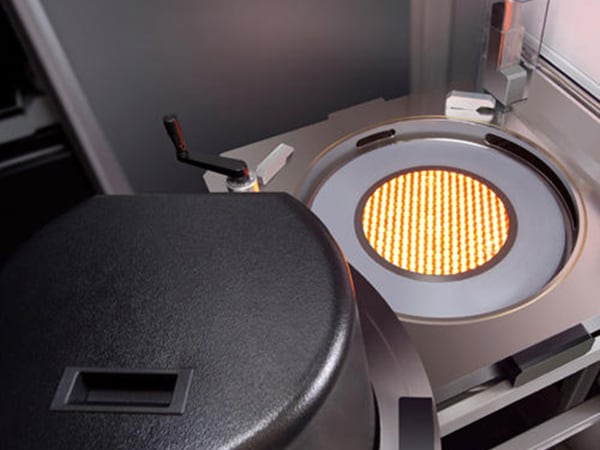
The Applied Vantage® Vulcan® RTP system is designed to provide industry’s best in class within die thermal pattern loading performance by utilizing a wafer backside lamp heating architecture. Within a die thermal pattern loading effects (PLE) are observed on certain device wafers and nodes due to temperature differences arising from die-to-die variations in radiant energy absorption. The Vantage® Vulcan® RTP system “turns down” its predecessor Vantage® Radiance® Plus RTP system’s multi-zone honeycomb lamp array, placing the lamp source onto the backside of the wafer to address these thermal pattern loading effects.
Together with addressing thermal PLE challenges, the Vulcan RTP system is designed to provide single wafer rapid thermal technology RTP enabling a wide temperature range of atmospheric spike anneals from 350°C to 1350°C. Combining world-class RTP chamber technology with a high-volume production-proven, low cost-of-ownership Vantage platform, the system’s streamlined design allows for shipment as a single unit, enabling quick install and faster start-up time to production.
The Vulcan RTP system leverages its predecessor’s technology that includes less than 1ppm O2 ambient control, a state-of-the-art temperature control system with proprietary pyrometry and emissometry design to enable precise high frequency closed loop temperature control for wafers with varying emissivities and a magnetically levitated high speed wafer rotation system for superior thermal wafer uniformity performance.
The Vulcan RTP “fast spike” quench enhances its spike anneal performance enabling advanced junction scaling and high-k metal gate reliability anneals for fast-performance, low-power-consumption devices in memory, logic, and foundry.
Key Features & Benefits
Multi-point in situ wafer temperature monitoring for best-in-class within-wafer and wafer-to-wafer uniformity
<1ppm O2 ambient control
<1.3s industry-standard sharp spike capability
Large thermal window to meet thermal budget for different anneal applications
Compact, high-productivity platform to maximize wafer output per footprint
- 1 / 3
- 2 / 3
- 3 / 3