Products & Technologies

Products & Services
Company
Contact
Back to Menu
Products & Services
Products & Technologies
Services
Resources
Company
Contact
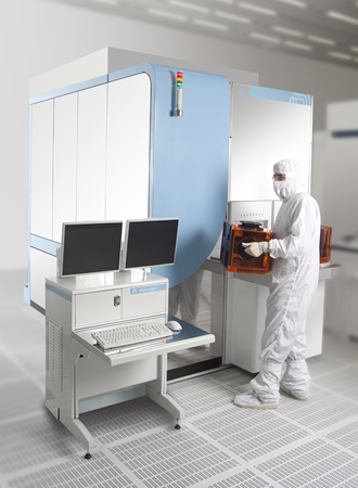
UVision® 8 Inspection
The UVision 8 system is the newest member of the successful UVision wafer inspection product family, featuring core technology of DUV laser illumination and full polarization control, with simultaneous dual channel (brightfield reflected light and grayfield scattered light) collection optics unique to this product line.
The system boasts the industry’s smallest optical inspection pixel size, which enables cutting-edge R&D and high-volume manufacturing with sub-10nm defect sensitivity. It also enhances defect inspection on advanced patterning layers in FEOL and BEOL applications for the 1xnm node, addressing technologies that include logic, DRAM, 3D NAND, double and quadruple patterning, and EUV layers.
The UVision 8 system features up to 10-fold improvement in light budget compared to the previous generation tool and additional unique imaging modes that enhance tool sensitivity by more than 50%. The platform is equipped with higher image processing power to enable up to two-fold improvement in throughput and better cost of ownership. Furthermore, the UVision 8 system runs on a new concept of operation that shortens recipe setup time by 50%.
In addition, the UVision 8 system incorporates Marker 2, the next generation of an integrated CAD-based application that combines customer regions-of-interest information and wafer characteristics based on customer needs. This capability enhances sensitivity while also boosting capture rates of prioritized defects of interest, enabling region-of-interest based binning, and tightening coordinate accuracy. The Marker 2 application is a key contributor to the new system’s value for process development and manufacturing.
The UVision 8 system is field-upgradable from the UVision 7 system, making its enhanced capabilities readily accessible to customers.