Products & Technologies

Products & Services
Company
Contact
Back to Menu
Products & Services
Products & Technologies
Services
Resources
Company
Contact
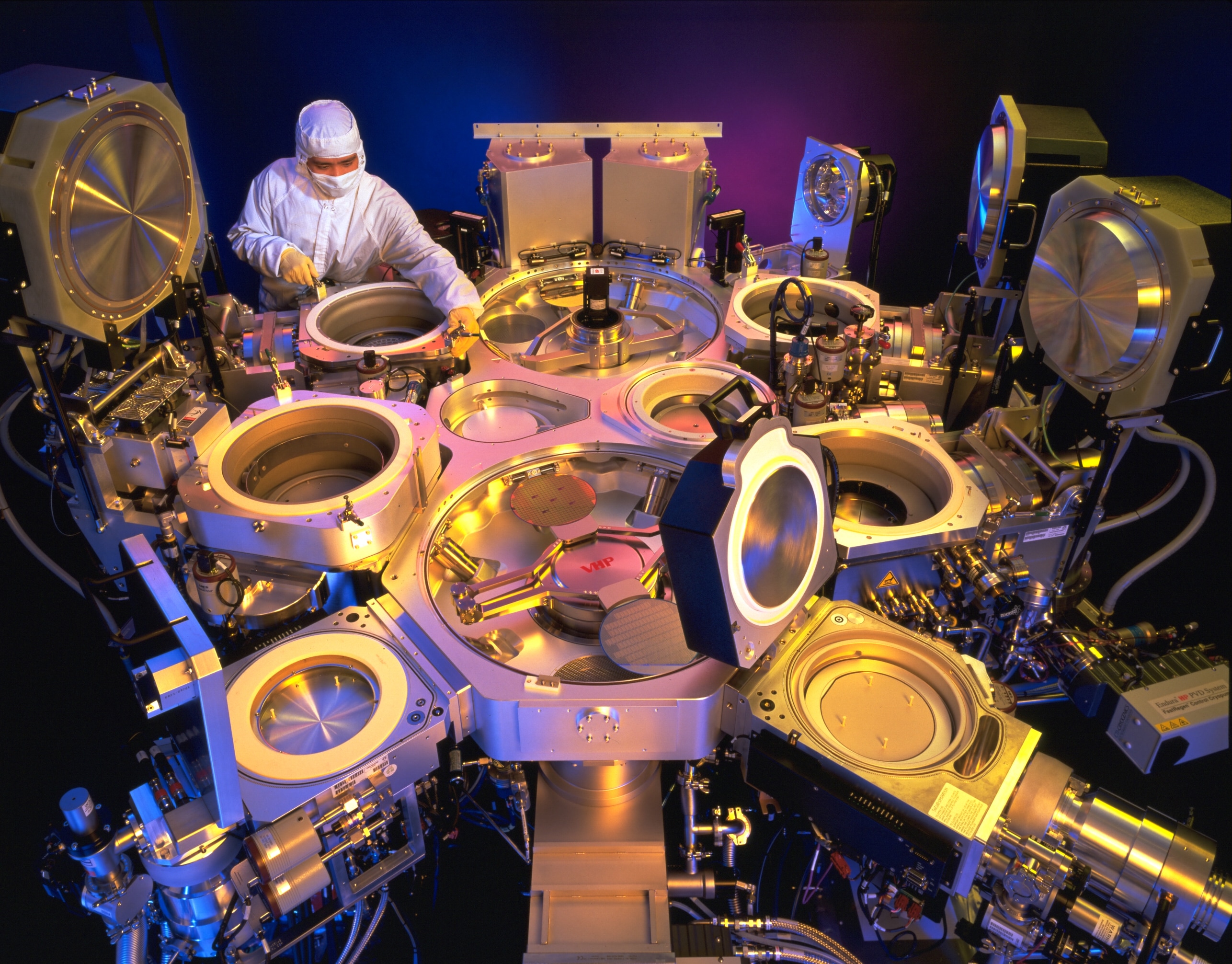
Endura® PVD
The Applied Endura platform is the most successful metallization system in the history of the semiconductor industry. With its deposition capabilities spanning front-end metallization, e.g., cobalt and tungsten; aluminum and copper interconnect; and packaging applications, e.g., underbump metallization, a vast majority of microchips made in the last 20 years have been created using an Endura system.
The system’s capacity to deposit a wide variety of ultra-pure films with tight control over film thickness, superior bottom coverage, and high conformality is key to the fabrication of leading-edge devices. Able to accommodate up to nine process chambers, including two preclean chambers for native oxide removal, the system offers the flexibility to mix and match chambers to create integrated multi-step process sequences.
Today’s 150mm and 200mm PVD challenges focus on depositing thicker, highly uniform, low-temperature films. Rapidly growing MtM applications, such as power devices, MEMS, RF, photonics, and packaging technologies, e.g., TSV, are driving PVD development in new materials, such as scandium doped aluminum nitride, lead zirconium titanate, aluminum nitride, indium tin oxide, aluminum oxide, and germanium, as well as new materials, including silicon carbide (SiC) and gallium arsenide.
With the introduction of a wide variety of MtM substrates, including SiC, wafer handling requirements have become especially demanding. The Endura platform is equipped with enhanced capabilities for handling transparent SiC wafers reliably and carefully from load lock wafer mapping to clear wafer orientation to wafer placement. Several hardware improvements are available to enhance process performance and tool productivity.