Products & Technologies
Products & Services
Contact
Products & Services
Products & Technologies
Services
Resources
Contact
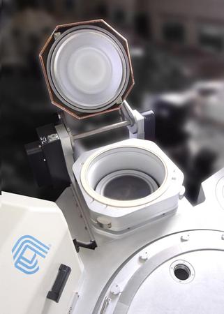
Endura® Avenir® RF PVD
As devices scale down, greater feature fragility and higher aspect ratios are making it more difficult for current PVD technology to fill narrow, deep structures and to avoid plasma damage. Using low-power, RF-based plasma minimizes the risk of damage and achieves more uniform plasma density distribution that results in better bottom coverage and uniformity.
The Endura Avenir system's RF PVD technology addresses high-k/metal gate applications as well as logic contact silicidation to 22nm and beyond.
For high-k/metal transistors, the Avenir system offers solutions for both gate-first and gate-last integration schemes, enabling chipmakers to transition easily between the two approaches. For gate-first, the RF PVD technology enables the controlled deposition of highly uniform and continuous thin films (<10Å). For gate-last, high-pressure, capacitively coupled plasma operation is used to ensure good bottom coverage and minimal overhang. The system's RF PVD technology also minimizes the risk of damage when depositing ultra-thin cap layers and metal gate films, delivering abrupt interfaces free of charge traps. The system’s tuning capabilities enable precise stoichiometric control of TiN films for overall Vt control without sacrificing film uniformity. In terms of effective work function, this requirement translates into <4.2eV for NMOS and >5.0eV for PMOS for high performance.
The RF PVD silicidation chamber doubles the bottom coverage obtained with conventional PVD Ni(Pt) processes, achieving more than 70% of the field thickness at the bottom of 5:1 aspect ratio features and uniform bottom coverage within feature and center-to-edge across the wafer. Uniform bottom coverage (3%, 1σ) translates into uniform resistance and lower leakage, while high platinum compositional uniformity translates into high device yield. The system delivers this performance at 30% lower cost of consumables than conventional PVD Ni(Pt) technology.
The production-proven Endura platform offers uniquely integrated capabilities for high-k/metal gate and logic contact silicidation applications. For gate applications, it offers the full range of PVD, CVD, and ALD technologies. For contacts, it combines the Siconi pre-clean, silicidation, and titanium nitride capping processes.